GCS offers InP HBT processes, which enable very high speed mixed-signal ICs both for test instruments and for 40-100G Transimpedance Amplifiers (TIAs) used in optical fiber communication applications. Two generations (4 processes) of InP HBT technologies have been developed with fT from 180 GHz to 300 GHz. Superior performance has been demonstrated by customers and qualified products have been in production since 2007.
| HBT Parameters |
|
SHBT1 |
DHBT1 |
DHBT2 |
DHBT3 |
DHBT3B |
| Emitter width |
(um) |
1 |
1 |
0.8 |
0.8 |
0.6 |
| Typical operating current density |
Jctyp (mA/µm2) |
1 |
1 |
2 |
2 |
2 |
| Maximum operating current density |
Jcmax (mA/µm2) |
2 |
2 |
3 |
3 |
3 |
| Typical operating voltage |
Vce (V) |
1 |
1.5 |
1.5 |
1 |
1 |
| Base-collector breakdown voltage |
BVcbo (V) |
6 |
8 |
5.5 |
4.5 |
4.5 |
| Collector-emitter breakdown voltage |
BVceo (V) |
3.5 |
7 |
4.5 |
3.8 |
3.8 |
| Emitter-base breakdown voltage |
BVebo (V) |
3.2 |
3.2 |
3.2 |
3.2 |
3.2 |
| Thermal resistance |
Rth (°C/mW) |
9.9 |
5.3 |
5.3 |
5.3 |
5.3 |
| fT (at max allowed operating current) |
(GHz) |
170 |
150 |
240 |
290 |
320 |
| fmax (at max allowed operating current) |
(GHz) |
200 |
180 |
200 |
250 |
330 |
| Passive Element Parameters |
Typical Value |
| TaN TFR Sheet Resistance (Ohm/sq) |
50 |
| MIM Unit Capacitance (fF/µm2) |
0.38 |
| MIM Capacitance Breakdown Voltage (V) |
- |
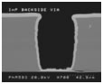
| Backside Vias |
Optional |
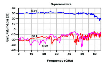
60 GHz TIA (courtesy of SMDI) |
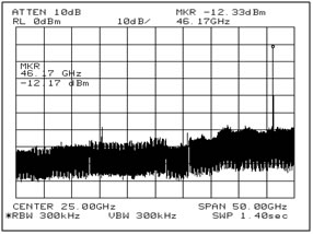
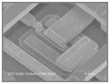
90 GHz Static Divider
(courtesy of Inphi Corp.) |